Flash memory is a type of non-volatile storage technology that can be electrically erased and reprogrammed. It is commonly used in memory cards, USB flash drives, and solid-state drives for general storage and transfer of data between computers and other digital products. Flash memory gets its name because it is designed to be erased in blocks, or “flashes.” So how does this complex technology actually work to store data reliably?
Flash Memory Basics
At the heart of a flash memory system are floating-gate transistors or cells. These are transistors that have an extra gate in between the control gate and the channel. This floating gate is electrically isolated, allowing it to store a charge for extended periods without leakage. Each flash memory cell is designed to hold one bit of data, represented by the presence or absence of charge on the floating gate. An uncharged floating gate represents a 1, while a charged floating gate represents a 0.
To write data to a flash cell, a high voltage is applied to the control gate and drain terminal, causing electrons to tunnel through the thin oxide layer onto the floating gate in a process called Fowler-Nordheim tunneling. The charge on the floating gate can be removed or erased by applying a negative voltage to the control gate, allowing electrons to tunnel back off the floating gate through quantum tunneling.
To read the data from a flash cell, a voltage is applied to the control gate and the channel current is sensed. If the floating gate is uncharged, the channel current will be high. If the floating gate is charged with electrons, the channel current will be low. This allows the state of the floating gate, representing a 1 or 0, to be determined.
Flash Memory Cells and Arrays
Individual flash memory cells are organized into large arrays or matrices for efficient data storage. The cells are arranged into rows and columns, with each cell mapped to a unique row and column address. In a typical flash chip, there can be thousands or even millions of individual cells in the array.
To select a specific cell for reading or writing, the appropriate row and column addresses are activated using peripheral decoder and driver circuitry. All the cells along an activated row or wordline have their control gates enabled, while a specific column or bitline is sensed to access just one cell. By rapidly selecting different row and column addresses, data can be efficiently read from or written to the array.
In addition to the main storage array, flash chips contain additional peripheral circuits for critical functions like sensing, programming, erasing, address decoding, voltage regulation, and interfaces. These peripheral circuits surround the core memory array and allow it to operate reliably.
Floating Gate Structure
The key innovation that enables flash memory is the floating gate transistor structure. As mentioned earlier, this is a special type of MOSFET transistor that has two gates – a control gate and a floating gate embedded between the control gate and the channel. The floating gate is completely surrounded by highly resistive dielectric material like silicon dioxide, separating it electrically from everything else.
Typically, the floating gate is made from a conductive material like polysilicon while the control gate is made from aluminum or other metal. When the floating gate has a high voltage applied, electrons can pass through the thin dielectric layer by quantum tunneling, allowing the floating gate to become charged or discharged. But with no voltage applied, the electrons remain fully trapped on the floating gate due to the excellent electrical isolation.
This allows the floating gate to act as a memory storage device, retaining a binary 0 or 1 indefinitely until it is rewritten. The presence or absence of electrons on the floating gate in turn affects the channel current flow when reading the cell. The floating gate essentially gives flash memory its non-volatile storage capability.
Single-Level vs Multi-Level Cells
Flash memory cells can be designed in two ways – as single-level cells (SLC) or multi-level cells (MLC). SLC flash can only represent one bit per cell, while MLC flash can store multiple bits per cell. Let’s look at how their designs differ:
- SLC – Each cell’s floating gate only needs to be charged or discharged, to represent a 1 or 0. This makes SLC the simpler and more reliable design.
- MLC – The floating gate can be partially charged to intermediate levels, allowing multiple bits to be stored based on the charge level. This increases density but reduce reliability.
The main advantage of MLC flash is greater storage density, since more bits can be stuffed into every cell. However, the tradeoff is lower write speeds and greater complexity in sensing multiple charge levels precisely during reads. MLC flash also wears out faster after repeated program-erase cycles. So SLC remains popular for applications requiring high reliability like industrial storage.
NAND vs NOR Flash
Flash memory arrays can be designed with either NAND-type or NOR-type connections between cells:
- NAND Flash – Cells are connected serially resembling a NAND logic gate. It provides higher density but slower random access.
- NOR Flash – Cells are connected in parallel resembling a NOR logic gate. It provides fast reads but lower density.
Here is a comparison between NAND and NOR flash:
| Characteristic | NAND Flash | NOR Flash |
|---|---|---|
| Cost | Lower | Higher |
| Density | Higher | Lower |
| Speed | Faster writes, slower reads | Faster reads, slower writes |
| Lifetime | Lower endurance | Higher endurance |
| Use cases | USB drives, memory cards, SSDs | Code storage, legacy systems |
As the table shows, NAND flash provides higher capacity storage at lower cost, making it ideal for data storage applications. NOR flash offers faster random reads, making it suitable for storing code.
Flash Memory Scaling
Flash memory capacity has scaled enormously over the years, allowing ever greater storage density. This is driven by scaling down the size of each memory cell through advances in semiconductor fabrication technology. As the cell size shrinks, more and more cells can be crammed onto a single silicon die.
Key developments that have enabled continued flash scaling include:
- Transitioning to smaller manufacturing nodes below 100 nm
- Moving from floating gates to charge trap structures
- Using Multi-Level Cell (MLC) and Triple-Level Cell (TLC) designs
- Stacking memory layers in 3D architectures
With cutting-edge fabrication processes, flash memory now offers terabyte-level storage capacity in tiny chip packages. 3D NAND flash in particular has enabled stacking of dozens of layers of memory cells for enormous density.
However, further flash scaling faces challenges like electron leakage and memory wearout issues. Novel technologies like resistive RAM and phase-change memory are being investigated as potential replacements to continue advancing non-volatile memory beyond the limits of flash.
Flash Memory Reliability
For any memory technology to be viable, it must reliably store data for extended periods over years of use. Flash memory uses a combination of clever circuit design and advanced error correction to achieve excellent data retention and endurance.
Here are some of the key reliability mechanisms used in flash storage:
- Error correction codes (ECC) – Powerful ECC schemes can detect and recover from many bit errors.
- Wear leveling – Writes are distributed across cells to avoid early wearout of frequently used blocks.
- Bad block management – Blocks that fail during use are detected and mapped out.
- Read scrubbing and healing – Periodic scans fix correctable errors before they accumulate.
Through these techniques, modern NAND flash storage can reliably store data for years with minimal data loss. However, flash memory cells still have a limited lifespan and will eventually wear out after ~10,000 writes.
Applications of Flash Memory
Thanks to its unique advantages like non-volatility, high density, fast writes and shock resistance, flash memory has become the storage medium of choice for a wide range of digital applications:
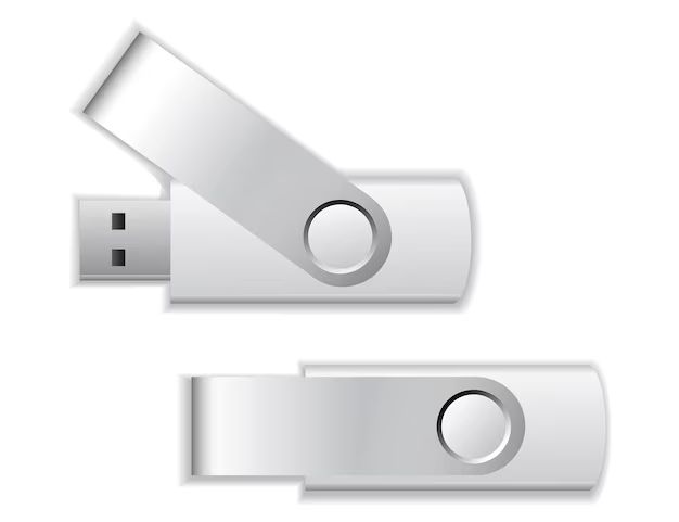
- USB Flash Drives – Portable flash storage for transferring and sharing data.
- Memory Cards – Flash-based storage for cameras, phones, consoles, etc.
- Solid State Drives (SSDs) – Fast flash-based replacement for hard disk drives.
- Tablets and Phones – Mobile devices rely extensively on flash storage.
- Flash-based Disk On a Chip – Flash used in embedded systems as disk replacement.
Flash memory has also enabled new product categories like USB drives, SSDs, and smartphones with vast storage capacities. The non-volatility and storage density of flash memory make it ideal for compact mobile devices and applications.
Manufacturing Process
Flash memory chips are fabricated in high-volume semiconductor fabrication facilities or fabs. The manufacturing process generally follows standard silicon CMOS logic technology with additional unique steps for the floating gate structure.
Here is a simplified overview of the flash memory manufacturing process:
- Start with a silicon wafer substrate – High purity, single crystal.
- Active area and isolation fabrication – Creates the transistor active areas and isolation trenches.
- Floating gate stack deposition – Layers that make up the floating gate are deposited.
- Gate patterning – Floating and control gates are etched and patterned.
- Peripheral CMOS fabrication – Additional transistors for logic are made.
- Contact and metallization – Backend steps to connect everything.
- Passivation and testing – Protective layer and electrical tests.
Hundreds of intricate fabrication steps are required to create the complex 3D floating gate structures with high precision and yield. State-of-the-art fabs are essential to manufacture the tiny flash memory cells required for high density and capacity.
Key Fabrication Steps
Let’s take a closer look at some of the most critical fabrication steps that enable flash memory technology:
- High-quality thermal oxide growth – The ultra-thin oxide layer surrounding the floating gate must be free of defects to retain charge.
- Doped polysilicon deposition – Precise control needed to dope the polysilicon floating gate and control gate.
- Ion implantation – Required for implanting the source and drain regions of each cell.
- Multi-layer metallization – For dense interconnects between the array and peripheral circuits.
Mastering these advanced steps enables the fabrication of high performance and reliable flash memory chips at extremely small geometries.
Conclusion
In summary, flash memory relies on transistors with floating gates that can be electrically charged to store data as 0s and 1s non-volatilely. Carefully engineered flash cells are arranged into dense arrays optimized for fast access. A mix of clever circuit and algorithmic techniques ensure flash memory is reliable for years.
Thanks to its unique advantages, flash memory has become the storage medium of choice for smartphones, tablets, memory cards and solid state drives. Continued technology scaling will enable flash memory to keep growing in capacity to meet the world’s exponential data storage needs for the foreseeable future.
