A solid-state drive (SSD) is a storage device that uses integrated circuit assemblies and flash memory to store data persistently without any moving parts [1]. SSDs evolved from early flash memory cards starting in the 1980s and gained mainstream momentum in 2007 when SSDs started displacing hard disk drives in laptops [2].
Compared to electromechanical disks like hard disk drives (HDDs) or floppy disks, SSDs are typically more resistant to physical shock, run silently, and have quicker access times and lower latency [3]. Today, SSDs come in several form factors and interfaces including SATA, PCIe, U.2, M.2, and NVMe. There are also different types of SSDs optimized for different use cases like SLC, MLC, TLC, QLC NAND for capacity vs endurance tradeoffs.
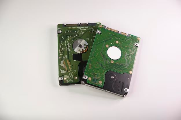
SSD Components
SSDs contain a few key internal components that work together to provide fast and reliable data storage. The main components in an SSD are:
- Controller – The controller manages all operations of the SSD and is similar to a microprocessor. It executes the firmware that governs the SSD’s operations and functionality. The controller interfaces with the host computer to receive/process requests and transfer data. Some SSDs have multi-core controllers for parallel operations and faster speeds. Controllers also incorporate error correction code (ECC) and wear leveling algorithms to ensure data integrity and maximize lifespan. Popular SSD controller manufacturers include Samsung, Phison, Marvell, Silicon Motion, Intel, and SandForce [1].
- NAND flash memory chips – NAND flash provides the raw storage capacity of the SSD. Multiple NAND flash chips are connected to the controller via channels. Common NAND flash types used in SSDs include MLC (2 bit per cell), TLC (3 bits per cell), QLC (4 bits per cell), and upcoming PLC (5 bits per cell) [2]. Higher bit NAND provides greater densities and capacities but lower endurance. NAND from well-known manufacturers like Samsung, Micron, SK Hynix, Intel, and Kioxia is prevalent.
- DRAM cache – The DRAM cache temporarily stores user data, mapping tables, and maintenance operations, allowing quicker access than NAND flash. It improves performance and lifespan by reducing the number of writes on the NAND flash. Cache sizes from 512MB up to several GBs may be present.
- Interfaces – The interface connects the SSD to the host computer and determines maximum bandwidth. Common SSD interface types include SATA, PCIe (NVMe), and M.2. NVMe offers the fastest interface speeds up to PCIe 4.0 x4 (4 lanes) throughput of nearly 8GB/s.
These components work in harmony to deliver responsive performance and robust data storage capabilities in SSDs.
[1] https://semiconductor.samsung.com/us/support/tools-resources/dictionary/semiconductors-101-part-3-inner-workings-of-the-ssd/
[2] https://www.storagereview.com/ssd-components
Manufacturing NAND Flash Memory
NAND flash memory is fabricated on semiconductor wafers that contain thousands of individual flash memory chips. The main manufacturers of NAND flash are Intel, Micron, SK Hynix, Samsung, SanDisk and Toshiba [1].
The fabrication process involves depositing and growing multiple thin film layers of materials on a silicon wafer using techniques like chemical vapor deposition. These layers form the control gates, floating gates, block oxide layers, and inter-poly dielectric of the NAND cells [2].
Dopants are implanted into the wafer to form the source and drain regions of each cell. Photolithography is used to pattern the layers and isolate individual cells. Etching removes excess material not covered by photoresist to form the NAND strings.
Once fabrication is complete, the wafers are diced into individual flash dies. These dies are then tested, packaged, and prepared for integration into SSDs and other devices.
Packaging the NAND Flash
One of the key steps in manufacturing SSDs is packaging the NAND flash memory. This involves inserting the bare flash dies into a circuit package to protect them and provide electrical connections.
The raw NAND flash dies are very small, fragile silicon chips produced on wafers. To package them, the dies are first separated from the wafer and undergo testing. The known good dies are then placed into a package, which protects the chips and connects them to a circuit board. Some common packaging methods include:
- TSOP (Thin Small Outline Package) – The flash die is enclosed in a thin plastic body with leads extending from the sides.
- BGA (Ball Grid Array) – The die is connected to a substrate with copper balls on the bottom, which are soldered to a PCB.
- CSP (Chip Scale Package) – A package nearly identical in size to the die, allowing high density.
The packaged NAND flash chips can then be soldered onto the SSD’s printed circuit board (PCB). Careful handling and electrostatic discharge protection is critical during packaging to avoid damaging the delicate flash dies.
Proper NAND flash packaging is essential for building a reliable SSD. It protects the storage medium and connects it to the rest of the device’s electronics.
SSD Controller
The SSD controller is the brain of the solid state drive, managing all of the crucial functions of the SSD. It is an embedded processor that executes firmware to handle communication between the NAND flash components and host system, while also carrying out other key operations like encryption, compression, error correction, and wear leveling (Sabrent). The controller architecture consists of the processor, flash interface, host interface, and DRAM interface.
The processor, often an ARM-based multi-core chip, runs the controller firmware and handles the computational tasks. The flash interface links the controller to the NAND flash memory and carries out functions like mapping between logical block addresses and physical locations on the flash. The host interface, such as SATA or PCIe, handles communication with the host computer. The DRAM interface links to the SSD’s DRAM cache that stores the firmware code, logical-to-physical mapping tables, and more (StorageReview).
Key responsibilities of the SSD controller and firmware include wear leveling to distribute writes evenly across the NAND flash, garbage collection to reclaim unused space from deleted data, bad block management, RAID configuration, encryption like AES-256, error correction, and more. The controller firmware is optimized over time through updates to improve performance and reliability.
Assembling the SSD
Assembling the SSD involves bringing together all of the components and connecting them together. This is a complex process that requires precision manufacturing.
The NAND flash memory chips are attached to the printed circuit board (PCB) through a process called solder reflow. This involves screen printing solder paste onto the PCB, then placing the chips and heating the entire assembly to melt the solder and form the electrical connections (The Process of How We Make SSD from a starting-to-finishing).
The controller chip is also soldered to the PCB. It is carefully positioned and oriented on the board. The enclosure is assembled, with the PCB and components placed inside. Interfaces like SATA or PCIe are added to enable communication with the host system.
At this stage, all the separate pieces of the SSD come together into one cohesive unit. The manufacturing process transitions from creating the individual components to integrating them together through meticulous assembly procedures.
Testing and Validation
To ensure the quality and reliability of SSDs, manufacturers perform various tests during and after the assembly process. Some key validation tests include:
Endurance testing verifies that the SSD can withstand its rated program-erase cycles before failing. Samples undergo intensive write cycles until they reach the end of their lifespan per the datasheet rating (ATP Inc.).
Performance testing checks the SSD’s read and write speeds, responsiveness, and other metrics using benchmark tools. Engineers validate that performance meets specifications across the full capacity (ScaleFlux).
Environmental stress screening submits drives to various temperature, vibration, and humidity conditions to confirm operation under normal and extreme environments.
Compliance testing validates that the SSD adheres to industry standards for electrical, EMI, and other parameters. Certifications like CE and FCC are earned through standardized test procedures.
Reliability testing includes long-term validation of error rate, data retention, power consumption, and other metrics critical to consistent SSD behavior over time.
Firmware Optimization
The firmware on an SSD handles important optimization tasks like garbage collection and wear leveling. Garbage collection helps recover unused pages so they can be rewritten. This is done by consolidating data to free up full blocks of storage. Wear leveling helps extend the lifespan of an SSD by distributing writes across all cells in the drive to prevent any single cell from wearing out too fast. The firmware needs to be optimized to perform these duties efficiently.
According to Crucial, SSD manufacturers release firmware updates to improve drive stability and performance. Updating to the latest firmware can help optimize garbage collection and wear leveling. For example, Samsung released a firmware update that adjusted garbage collection thresholds to be more efficient.
Windows also has built-in optimization like TRIM that works with the SSD firmware. As explained by Auslogics, TRIM tells the SSD which blocks of data are no longer in use and can be wiped and reused. This improves performance by reducing fragmentation.
Adding Interface and Enclosure
Once the SSD has been fully assembled and tested, it is ready to be installed into an enclosure to provide connectivity through a common interface. Popular enclosures provide connections such as USB, Thunderbolt, or PCIe which allow the SSD to be used externally or installed internally in a computer system.
To install the SSD in an enclosure:
- Select an appropriate SSD enclosure that matches the physical form factor and interface of the SSD. M.2 and 2.5″ enclosures are common choices.
- Open the enclosure and insert the SSD into the slot, ensuring it is fully seated.
- Secure the SSD with any provided screws or brackets.
- Attach any interface cabling such as USB or Thunderbolt to the enclosure.
- Optionally install the enclosure into a computer system if using an internal mounting format.
Once physically installed, the enclosure provides a standard connectivity interface to allow easy usage of the SSD. Enclosures commonly use high-speed interfaces like USB 3.2 Gen 2×2 (20Gbps) or Thunderbolt 3 which can fully utilize the SSD’s capabilities.
Some examples of popular SSD enclosures supporting the latest high-speed interfaces include the SSK Aluminum M.2 NVME SATA SSD Enclosure and the M.2 NVME SATA SSD Enclosure Adapter.
Final Verification
Before an SSD can be shipped to customers, it undergoes extensive final verification and quality assurance testing. This phase ensures the SSD meets strict specifications and performs as intended. Some key steps in final verification include:
Testing interface protocols and speed – The SSD is connected to test systems via SATA, PCIe, NVMe, etc. to validate interface operation and benchmark transfer speeds. It must achieve maximum rated performance.
Validation of thermal design – Test systems monitor SSD temperature across various workloads. Cooling mechanisms must keep the drive within safe operating ranges.
Final firmware optimization – Firmware is updated and tweaked as needed to optimize performance, compatibility, reliability, power efficiency, and features.
Stress testing – The SSD undergoes prolonged stress testing with heavy workloads well beyond normal usage. This verifies robustness and detects any latent defects.
Life cycle testing – The SSD is subjected to simulated aging through extensive program/erase cycles. It must retain data integrity throughout its rated endurance.
Environmental testing – The SSD experiences varied temperature/humidity, shock/vibration, and other environmental conditions. It must withstand the rigors of real-world use.
Compliance testing – The SSD is validated against regulatory standards like FCC, CE, UL, RoHS, and others. It must satisfy all mandated requirements.
Final quality audit – QA team performs final checks at each manufacturing step. The finished SSD must meet all specifications before shipment.
These rigorous verification tests validate overall SSD reliability and fitness. Passing final verification clears the SSD for customer delivery.
