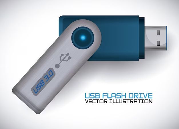
Universal Serial Bus (USB) storage devices have become ubiquitous for portable data storage and transfer. From small thumb drives to external hard drives, USB storage allows users to easily store, access and transport files across devices. But what exactly is inside these handy devices that makes data storage and transfer possible? Here we will explore the internal structure and components that give USB storage its functionality.
How Does USB Storage Work?
At its most basic, a USB storage device consists of flash memory chips and a USB controller chip enclosed in protective casing. The flash memory chips store the actual user data, while the controller chip manages the storage and transfer of this data between the flash memory and the USB port on a computer or other device.
Flash memory contains arrays of floating gate transistors that retain data even when power is removed. Storing data involves charging these floating gates to represent binary 1s and 0s. Flash memory comes in forms like NOR and NAND, with NAND being the most commonly used in USB drives due to its higher storage density.
The USB controller chip converts the parallel data from flash memory into serial data that can be sent over the USB protocol. It also manages tasks like block addressing, error correction, wear leveling and write protection to optimize performance and device lifetime. The controller presents the flash memory to the host device as a set of logical block addresses that can be read and written like a disk drive.
USB Interfaces
There are several USB interfaces that are, or have been, common in USB storage devices:
- USB 1.1 – Original USB standard, capable of speeds up to 12 Mbit/s (Slow for most current uses)
- USB 2.0 – Faster USB standard from 2000, with speeds up to 480 Mbit/s
- USB 3.0/3.1 Gen 1 – Introduced in 2008, up to 5 Gbit/s transfer speeds
- USB 3.1 Gen 2 – Launched in 2013, up to 10 Gbit/s transfer speeds
- USB 3.2 – Current standard launched in 2017 with two generations: Gen 1 (5 Gbit/s) and Gen 2 (10-20 Gbit/s)
- USB4 – Next generation standard launched in 2019, up to 40 Gbit/s based on Thunderbolt 3 protocol
The USB interface versions indicate the maximum potential data transfer rates between the flash storage and host device. For example, a USB 2.0 drive will be limited to 480 Mbit/s transfers, while a USB 3.2 Gen 2 drive can theoretically transfer data up to 20 Gbit/s, which is around 2.5 GB/s.
USB Connector Types
In addition to interface versions, USB storage devices come with various physical connectors to plug into host ports. These include:
- Type-A – Rectangular USB port/plug found on host devices
- Type-B – Square-shaped port on USB printers and other large peripherals
- Mini-A/Mini-B – Smaller versions of Type-A/Type-B on smaller devices
- Micro-A/Micro-B – Even smaller connectors for phones, digital cameras, etc.
- USB-C – Emerging standard with oval port that can support higher speeds
The Type-A connector is by far the most common for USB storage devices designed to plug into computers and consumer electronics. However, USB-C is gaining popularity as a future standard due to its small size, high speeds, and reversible plug orientation.
Typical Internal Components
If you were to take apart a USB flash drive or external hard drive, you would likely find these core components inside:
- USB Controller Chip – Controls the interface between flash storage and USB port. May include wear leveling, error correction, encryption, etc.
- NAND Flash Memory Chips – Stores user data. Multiple chips provide more capacity.
- Crystal Oscillator – Provides clock signal to synchronize operations.
- LEDs – Indicator lights for drive status and activity.
- Voltage Regulators – Provides stable voltage supply to components.
- Resistors/Capacitors – Helper components for managing current and voltage.
Higher capacity USB drives may include a SATA bridge chip to translate the SATA interface of larger NAND flash chips. External hard drives also contain a separate hard disk drive inside that connects to the USB bridge chip.
Main Firmware Components
The USB controller chip runs firmware to handle tasks like:
- USB Mass Storage Class – Allows OS to interface with drive as a generic block storage device
- Flash Translation Layer – Maps logical addresses to physical addresses on NAND flash memory
- Wear Leveling – Distributes writes across flash cells to extend lifespan
- Bad Block Management – Detects and maps out failed flash memory regions
- Encryption – Optional AES encryption to secure stored data
- File System – Manages file storage on flash memory (FAT32, exFAT, etc.)
In many USB drives, the firmware is provided by the manufacturer of the controller chip. However, some vendors utilize custom firmware for added functionality.
Inside a USB Thumb Drive
As a specific example, here are the typical internals of a common 32GB USB 2.0 flash drive:
- USB 2.0 Controller Chip
- NAND flash memory chip(s) with total 32GB capacity
- Crystal oscillator clock chip
- LED indicator light
- USB Type-A male connector
- Printed circuit board (PCB)
- Plastic casing
At the core, one or more NAND flash memory ICs provide the 32GB storage capacity. A USB controller chip manages the interface and data transfer via the USB 2.0 protocol. Other inexpensive components provide supporting functions like clock timing and activity indicators.
While 32GB is on the higher side for a single flash memory chip currently, many drives stack multiple dies in the same package to reduce cost. The small physical size allows the PCB, connectors, and other parts to fit inside a compact plastic case around the size of a thumb.
Inside a High-Capacity External Hard Drive
For larger external USB hard drives with capacities up to 10TB or more, the internal structure is considerably different than portable flash drives:
- USB 3.0/3.1/3.2 controller chip
- SATA bridge chip
- Full-size 3.5″ HDD (Hard Disk Drive) mechanism
- AC power adapter and circuitry
- External case with USB 3.0 port
Rather than NAND flash chips, these drives use a standard hard disk drive inside that can come in large capacities up to 10TB. This connects via a SATA adapter to a USB 3.0 controller chip.
Larger electronics components are required to support the HDD mechanism and power supply. The outside case also needs to enclose the full HDD unit and PCBs while enabling airflow and heat dissipation.
How is USB flash storage manufactured?
USB flash drives and SSDs undergo a multi-stage manufacturing process with both automated and manual assembly required. Here is a general outline of the key stages:
- Wafer Fabrication – The NAND flash memory and controller chips start as silicon wafers fabricated in a semiconductor cleanroom.
- Die Cutting – The wafer is precision cut into hundreds of individual flash memory and controller dies.
- IC Packaging – The dies are assembled into plastic or ceramic IC packages or packages-on-package.
- SMT Assembly – The ICs and other components are surface mounted onto the PCB in an automated SMT line.
- Device Assembly – The PCB is inspected and assembled into the outer USB casing, sometimes involving manual steps.
- Firmware Loading – Software that operates the controller chip is loaded onto the device.
- Final Testing – Quality assurance testing confirms device meets specifications.
For USB drives with packaged NAND flash chips, the packaging stage puts multiple dies into a single BGA package. The automated SMT assembly efficiently solders the chips and other components onto the PCB.
While equipment can assemble the PCB and casing, manual labor helps create a polished final product. The firmware loading and testing requires specialized software utilities.
Common USB Storage Device Standards
USB storage devices adhere to core standards that enable compatibility between vendors. These include:
- USB Specification Standards – Such as USB 3.2 which defines connectors, cables, protocols, etc.
- USB Mass Storage Class – Driver interface to allow USB storage to connect to host machines.
- USB Attached SCSI Protocol (UASP) – Optional SCSI command implementation for better performance.
- NVM Express (NVMe) – Interface protocol designed for high speed PCIe SSDs.
- JEDEC Standards – Defines interface requirements for NAND flash memory chips.
Compliance with standards like USB 3.2 and Mass Storage Class allows devices made by different manufacturers to work consistently when plugged into computers and other USB hosts. Emerging standards like UASP and NVMe aim to optimize data transfer speeds as technology advances.
File Systems for USB Storage
USB storage devices format their flash memory into standard file systems that operating systems recognize. Common file systems include:
| File System | Maximum Individual File Size | Maximum Volume Size | Introduced |
|---|---|---|---|
| FAT12 | 4 GB | 32 MB | 1977 |
| FAT16 | 2 GB | 2 GB | 1984 |
| FAT32 | 4 GB | 2 TB | 1994 |
| exFAT | 16 EB | 128 PB | 2006 |
| NTFS | 16 EB | 256 TB | 1993 |
Older/smaller USB drives may use FAT16 or FAT32, which have more limitations. Modern USB drives often use exFAT for its large file size and volume support. NTFS is common on larger external USB hard drives formatted for Windows. These file systems organize data on the flash memory and present it to the host OS.
Typical Data Transfer Speeds
The interface version and actual flash memory performance determine the real-world data transfer speeds for a USB drive. Some typical speeds include:
- USB 2.0 – Up to 35 MB/s read, 10 MB/s write
- USB 3.0 – Up to 625 MB/s read, 500 MB/s write
- USB 3.1 Gen 2 – Up to 1000 MB/s read/write
- USB 3.2 Gen 2×2 – Up to 2000 MB/s read/write
There is variance among individual drives, but USB 3.2 Gen 2×2 with fast NAND flash has the potential to reach nearly 2 GB/s. However, the USB port it connects to also needs to support this latest standard.
Why are read speeds faster than write speeds?
On most USB flash drives, read speeds are significantly faster than write speeds. There are a few factors contributing to this difference:
- NAND flash can be read in parallel vs writes require sequential operations.
- Additional steps like erase and error checking occur on writes.
- USB uses bulk transfer mode which favors reading.
- The USB controller has a smaller buffer for writes compared to the read buffer.
Optimizing the controller firmware and flash memory can help close the gap between reads and writes. But in general, the asymmetric operation of NAND flash leads to faster data access compared to data storage.
Durability and Lifespan
USB flash storage can withstand reasonable shock, vibration, and pressure thanks to solid-state memory lacking moving parts. However, there are still limits to the device durability:
- Shock: 1500Gs operating, up to 5000Gs non-operating
- Vibration: 60Gs operating, 300Gs non-operating
- Altitude: -50 to 10,000 ft operating
- Estimated lifecycles: 100,000 to 1 million writes per cell
Carefully engineered casing protects the internal components during drops and vibration. The tight flash memory tolerances prevent data errors under normal environmental conditions.
NAND flash endurance is limited, but modern techniques like wear leveling distribute writes across more cells to extend the total lifetime. High-end drives may last for decades even with heavy usage.
Security Features
USB drives handle sensitive data, so security is an important consideration. Some integrated features include:
- Password Protection – Password must be entered to access drive contents after connecting.
- Hardware Encryption – Encrypts all data stored on the drive via AES or similar algorithms.
- Read-Only Modes – Allows locking drive as read-only to prevent writing new data.
- Tamper-Resistant Casings – Detects physical tampering attempts.
- Biometrics – Fingerprint readers or other biometrics can unlock access to stored data.
These types of protection prevent unauthorized access if the drive is lost or stolen. Software encryption, available on most operating systems, can also be used in conjunction with the built-in security features.
Conclusion
USB flash drives may appear like simple data storage devices, but they contain sophisticated internals optimized for portability, capacity, speed, and durability. Components like the USB controller, NAND flash chips, and firmware create a compact solid-state drive with no moving parts. Standards compliance allows reliable plug-and-play usage across many devices while advancing interfaces provide sequentially faster data transfer capabilities. USB drives are an excellent example of how mature electronics manufacturing can produce a robust, useful product in a miniature form factor.